0x0000  47 4D 53 20 4C 4F 54 38
0x0010  38 34 31 32 2D 30 37 00
0x0191  4D 41 50 20 01 01 03 01
0x01A1  01 01 FF 01 01 03 01 01
Wafer map intelligence — on-prem
Read the wafer.
MAPx parses E142, KLARF, SINF, TEL, TFF, XYBin, and STDF natively, renders every die, and runs the spatial analysis your yield meeting needs — on your servers, next to your MES.
7 FORMATS · NO CONVERTERSON-PREM DEPLOYMENTMES-READY
THE PROBLEM
Your yield data speaks seven languages.
The tester writes STDF. The prober writes TEL GMS. Inspection writes KLARF. The OSAT sends SINF. Your MES wants E142. And the converter script holding it together was last touched in 2019.
FileVersion 1 8;
FileTimestamp 03-11-26 09:41:22;
LotID "LOT-88412";
WaferID "07";
DefectRecordSpec 9 DEFECTID X Y ...;
DEVICE:MPX2-0704A
LOT:LOT-88412
WAFER:07
ROWCT:44
COLCT:52
<SubstrateMap SubstrateId="LOT-88412.07">
  <BinCodeMap NullBin="FF"
      BinCodeType="HexaDecimal">
    <BinCode>01 01 03 01 FF 01</BinCode>
</BinCodeMap>0x0000 54 46 46 02 00 00 10 27 0x0020 43 4F 57 00 E8 03 00 00 0x0040 D2 04 00 00 4C 4F 54 38 0x0060 38 34 31 32 07 00 01 00
x,y,bin
-12,4,01
-11,4,01
-10,4,07
-9,4,01
0x0000  02 00 00 0A 02 04 8E 00
0x0020  01 0A 4C 4F 54 38 38 34
0x0040  02 0A 07 00 57 30 37 00
0x0060  05 14 01 00 07 00 F4 FF
The bottleneck isn't your analysis.
It's the plumbing.
01 · INGEST
Drop the converter.
MAPx reads and writes every format on the floor, natively. No third-party converters, no per-format licensing.
02 · RENDER
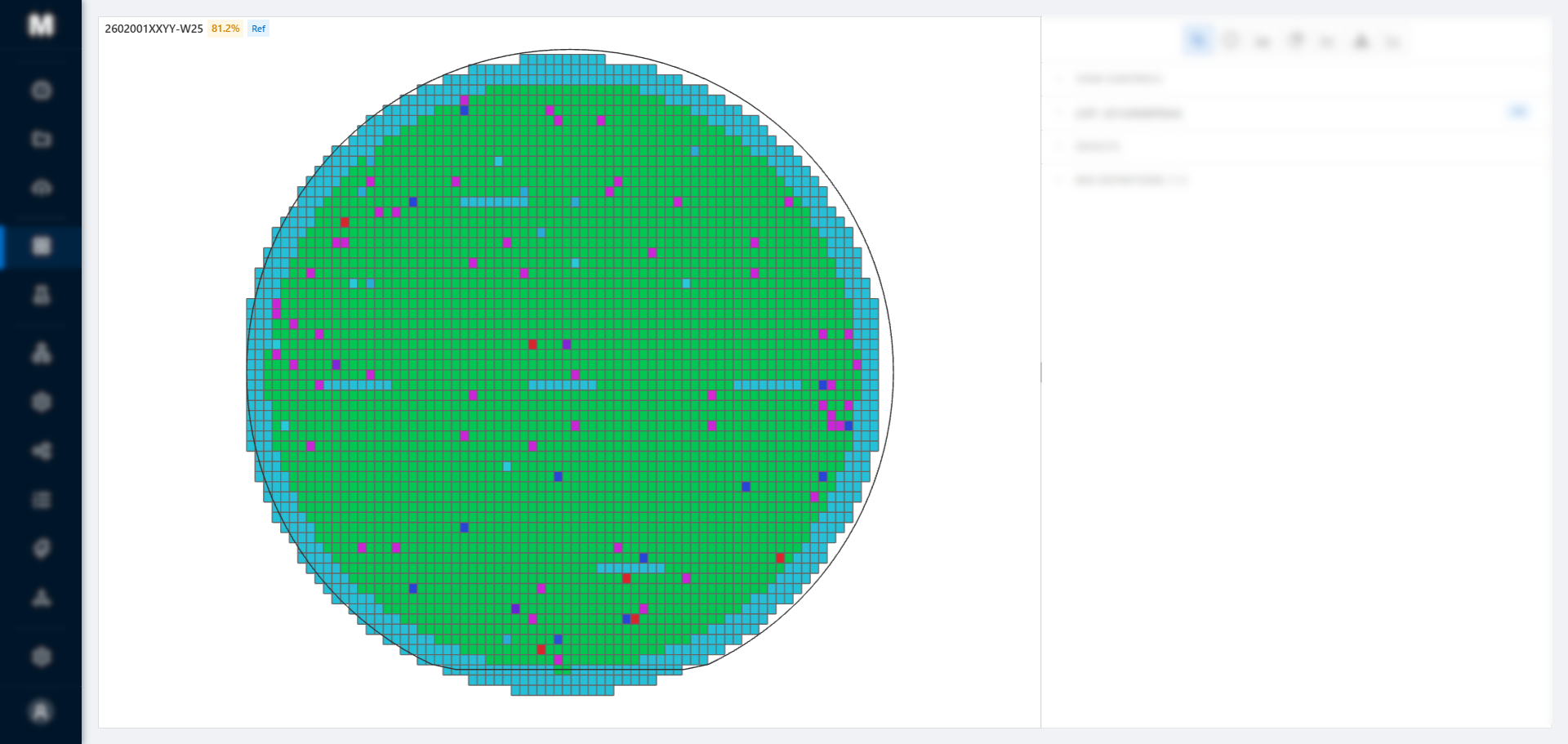
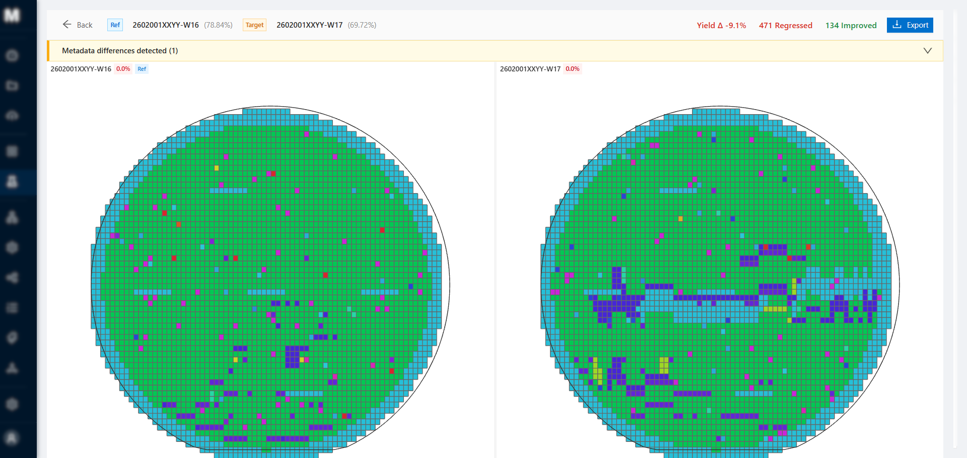
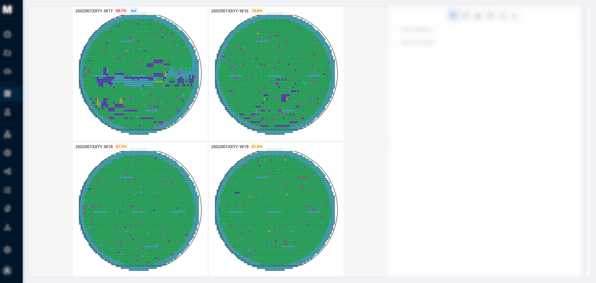
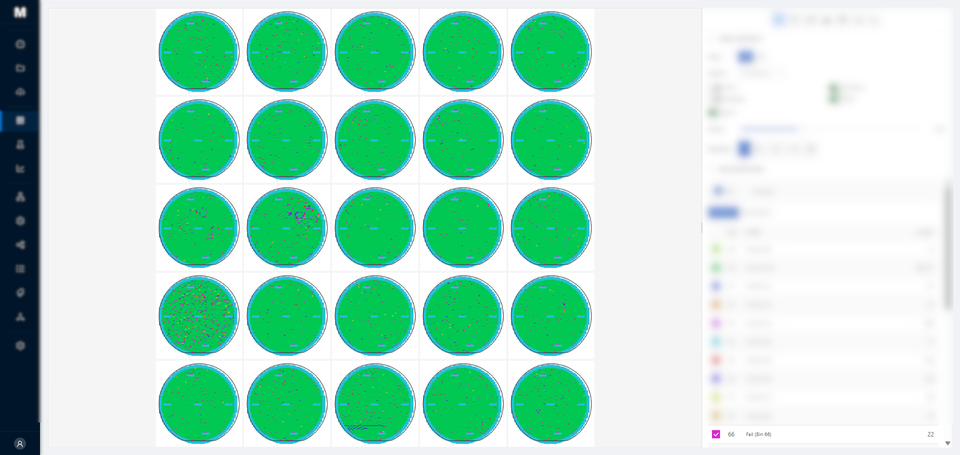
One wafer in full detail. Or the whole lot at a glance.
Every die rendered, every bin coded, side-by-side comparison and lot-level grids — the product screenshots below are the real viewer.
03 · ANALYZE
A ring is a process.A scratch is a handler.A repeat is the reticle.
Spatial patterns carry causes. MAPx finds the pattern and points at the process step.
Zonal analysis
Yield by radial and angular zones. A vague edge problem becomes a numbered zone with a fail rate.
GDBN screening
Good dies in bad neighborhoods, flagged before they ship.
Cluster detection
Connected-region labeling separates systematic clusters from random noise, with size and location per cluster.
PAT
Part average testing marks dies that pass spec but sit outside the population.
Reticle analysis
Folds the map onto the reticle grid. A defect that repeats in the same field position is a mask problem, not a process one.
AI signature classification
A deep learning classifier trained on large-scale production wafer maps names the failure pattern — ring, scratch, donut, edge loss — with a confidence score. Inference runs on-prem; no data leaves the fab.
04 · ACT
Fix the map. Feed the line.
Analysis that ends in a file the line can consume, not a screenshot.
Edit and write back
Interactive die editing with full undo/redo. Export the corrected map as E142, SINF, TEL, or XYBin.
MES-ready
Corrected maps export in the standard interchange formats an MES already ingests — no manual re-entry between analysis and dispatch.
On-prem, full stop
Your substrate data never leaves the fab network. No cloud dependency, nothing calls home.
PROBERMAPx (ON-PREM)MES
Release log
v1.3.0STDF IngestAugust 2026
Native ingest of STDF — the binary datalog wafer sort testers write. One datalog fans out to every wafer it contains, with both hard bin and soft bin carried through to the map.
Format Support
- STDF V4 binary datalog (read)
- Multi-wafer datalogs split into individual maps
- Hard bin and soft bin both retained
- Automatic detection alongside the existing formats
Large-File Handling
- Datalogs streamed at ingest, never loaded whole
- Gigabyte files supported without a memory penalty
- Map views stay fast regardless of source size
Test Data
- Per-die parametric drill-down on demand
- Lot, wafer, and tester metadata preserved
- Source format reported honestly — never relabelled
v1.2.0AI Defect ClassificationMay 2026
Deep learning classification of wafer spatial signatures. Every ingested substrate is automatically labeled with its defect pattern — running fully on-premises.
Deep Learning Model
- Trained on large-scale real production wafer maps
- High classification accuracy, validated on industry-standard benchmarks
- Robust to wafer rotation and orientation variation
- CPU inference — no GPU required
Signature Classes
- Center, Donut, Edge-Ring, Edge-Loc
- Localized, Scratch, Random, Near-Full
- Multi-label detection for mixed patterns
- Confidence score per classification
Automation
- Automatic classification on ingest
- Batch re-classification across lots
- Low-confidence results flagged for review
Deployment
- Fully on-premises inference
- No cloud dependency — data never leaves the fab
- Runs inside the existing MAPx worker service
v1.1.0GDBN AnalysisFebruary 2026
Spatial reliability screening to identify good dies at risk in failing neighborhoods. Supports single substrate and batch processing.
Screening
- Neighborhood-based spatial screening
- Configurable risk thresholds
- Yield loss safeguard
- Edge die handling
Batch Processing
- Multi-substrate analysis
- Consistent screening across lots
- Summary statistics
Visualization
- Interactive risk heatmap
- Score distribution histogram
- Flagged die overlay
Export
- Flagged die results export
- Audit-ready reporting
- Industry standards compliance
v1.0.0Initial Production ReleaseFebruary 2026
Substrate result management system with universal format support, interactive visualization, automated failure analysis, and wafer map editing.
Format Support
- E142, KLARF, SINF, TEL, XYBin
- Bidirectional read and write
- Automatic format detection
- No third-party converters required
Visualization
- 2D and 3D interactive wafer maps
- Multi-map side-by-side comparison
- Customizable die markers and overlays
- Pan, zoom, and rotation controls
Analysis
- Pairwise map comparison
- Automated failure cluster detection
- Spatial pattern analysis
- Bin transition tracking
Editing & Export
- Interactive die bin editing
- Full undo and redo support
- Optimized incremental save
- Industry-standard format export
OPEN BENCH
The open bench.
Free engineering tools that run entirely in your browser. No signup, no upload — your data stays on your machine.
Flagship
Wafer Map Editor
Paint pass and fail bins on 150, 200, and 300 mm wafers. Defect pattern generators, full undo and redo, autosave — and the whole map fits in a share URL.
150 / 200 / 300 mm · patterns · undo/redo · share by URL
CONTACT
Bring us your hardest wafer map.
Send a sample file and the question you need answered. You'll hear back from the people who wrote the parsers.